Page 2 of 3
Posted: 04 Nov 2012, 09:28
by 7bit
Soarer wrote:...
That might take you 30 minutes once you know the basics of the tools. How long to write the script? Yeah, now how long to write a script that copes with special cases, even just non-full columns/rows? And don't miss out the time it takes you to figure out what the script should be writing

At which point exporting the netlist and importing it to pcbnew should give you a massive stack of components all in the same place. THEN you can think about a script to place the switches. This is the only part I think worth scripting.
I dunno if you're planning on using diodes inside the switches or placing them seperately... if it's the former then I doubt that SW_PUSH is the best choice for the schematic symbol; a custom MX with diode symbol would be better.
Thanks for the list.
Switch placement: To place them manually is quite a pain, especially because there are so many variants.
Doing this from one source is much more pleasant. So the only thing that is remaining is drawing the tracks.
edit: placing the components on the PCB is plain sailing, because all I have to do is copy the modules from the modules file and set their name and position on the PCB, both are well-known.
Posted: 09 Nov 2012, 08:56
by 7bit
Steps to be performed after running the PCB-generating script on mypcb:
- select current path in Preferences/Library: Hit Add in the 2nd field and enter $PWD/
- "use relative path?": Hit "yes"
- In 1st field hit Add and select "components.lib".
- save the useless config file (which is ignored even if loaded!)
- Now hit 4th icon from the right (Netlist generation) in the top panel of the main window.
- hit Netlist
- and save the file.
- eeschema can be closed now.
- select current path in Preferences/Library: Hit Add in the 2nd field and enter $PWD/
- "use relative path?": Hit "yes"
- In 1st field hit Add and select "mypcb.mod".
- save the useless config file (which is ignored even if loaded!)
- Now hit 2nd icon from the right (read Netlist) in the top panel left of that useless "+/- to switch" field of the main window. (look at the baloon texts).
- hit read current netlist
- ignore all warnings
- now you can place the traces....
Posted: 24 Nov 2012, 20:01
by 7bit
Next question:
How to export the PCB design into something like this:

I only get a very un-smooth postscript file (via print to file).

Posted: 25 Nov 2012, 03:22
by bpiphany
That one is generated from gerbv, KiCAD is really poor on exporting image files...
Posted: 25 Nov 2012, 09:42
by 7bit
bpiphany wrote:That one is generated from gerbv, KiCAD is really poor on exporting image files...
Thanks!
Now, how do I export the file to read with gerbv?

Posted: 25 Nov 2012, 17:15
by bpiphany
That is something absolutely central, this you've got to learn. The gerber files is what this is all about. File->Plot, and from there you should be able to figure things out =)
Posted: 25 Nov 2012, 17:25
by 7bit
bpiphany wrote:That is something absolutely central, this you've got to learn. The gerber files is what this is all about. File->Plot, and from there you should be able to figure things out =)
Exactly at this point nothing works anymore. Pcbnew spits out a lot of files and when I run gerberv on them nothing happens...
Posted: 25 Nov 2012, 18:55
by bpiphany
"Open with" doesn't work with gerbv, the program only starts without loading the file. It usually sets the folder to the correct one when you want to open the file from within the program again... And to add the gerber files to the current project, you need to use the plus button at the bottom of the left hand panel.
Posted: 25 Nov 2012, 20:15
by 7bit
Code: Select all
HyperMini_PCB-Adhes_Back.gba
HyperMini_PCB-Adhes_Front.gta
HyperMini_PCB-Back.gbl
HyperMini_PCB-Comments.gbr
HyperMini_PCB-Drawings.gbr
HyperMini_PCB-Eco1.gbr
HyperMini_PCB-Eco2.gbr
HyperMini_PCB-Front.gtl
HyperMini_PCB-Mask_Back.gbs
HyperMini_PCB-Mask_Front.gts
HyperMini_PCB-PCB_Edges.gbr
HyperMini_PCB-SilkS_Back.gbo
HyperMini_PCB-SilkS_Front.gto
HyperMini_PCB-SoldP_Back.gbp
HyperMini_PCB-SoldP_Front.gtp
Which is the file I must load?
When I run
it does not work.
Posted: 25 Nov 2012, 21:48
by bpiphany
I suggest
and then do it through the GUI ;)
Edit: actually, the following worked perfectly for me =D
But you still probably want to set specific colors to different layers, sort them in a specific order, and save a project file with those settings until next time...
Edit again: Depending on which version of KiCAD you are using you may want to tick the "use minimal header" in the plot dialogue. I think gerbv used to crash for me otherwise... In my new version of KiCAD i think they use the minimal header and did away with the check box.
Posted: 26 Nov 2012, 21:08
by 7bit
It works with your Phantom files, but not with my stuff.
Is the gerbv-thing in any way important, or just cosmetic?
Code: Select all
(gerbv:18946): GLib-GObject-WARNING **: value "-nan" of type `gdouble' is invalid or out of range for property `position' of type `gdouble'
This is one line of the error messages which cause my input files.
edit: It seems there is something missing.
Posted: 26 Nov 2012, 21:59
by 7bit
OK, problem solved!

The frame was missing. It does not matter where the elements are, but there must be a frame:
Code: Select all
$DRAWSEGMENT
Po 0 132500 -3000 -3000 -3000 150
De 28 0 900 0 0
$EndDRAWSEGMENT
$DRAWSEGMENT
Po 0 132500 44000 132500 -3000 150
De 28 0 900 0 0
$EndDRAWSEGMENT
$DRAWSEGMENT
Po 0 -3000 44000 132500 44000 150
De 28 0 900 0 0
$EndDRAWSEGMENT
$DRAWSEGMENT
Po 0 -3000 -3000 -3000 44000 150
De 28 0 900 0 0
$EndDRAWSEGMENT
Posted: 27 Nov 2012, 20:47
by bpiphany
7bit wrote:OK, problem solved!
:ugeek:
The frame was missing. It does not matter where the elements are, but there must be a frame:
That seems a bit odd. I don't see why you shouldn't be able to draw a PCB without specifying the edges...
Gerbv is good to have to look at the gerber files. KiCAD has a gerber viewer as well, but I haven't used it much. So I can't tell if it is any good =)
You should read up on the gerber file format. It's really simple, and when you've learned it, you can script the gerber files directly ;)
http://www.ucamco.com/LinkClick.aspx?fi ... nload=true
Posted: 27 Nov 2012, 22:14
by 7bit
Wait!
You mean I don't need the stuff I already done and have to start anew with the gerber files?!

One more thing: How do I add vias?
Posted: 29 Nov 2012, 20:57
by 7bit
2 more questions:
1. How to add vias?
Answer: Click on a trace and then left click to select Place Via.
2. How to change the width of traces?
It is obvious that the traces must be less wide, because the soldering points of the ATMEGA32WHATEVER are too close to each other.
Still need to know how narrow the tracks can be.
Posted: 29 Nov 2012, 22:54
by bpiphany
You can add your own trace widths under Design rules. To place a via you press PgUp/PgDn while drawing a trace. There is a list of all hotkeys that is probably useful. To change trace width you can right click and go through that menu.
The manufacturer probably have specifications on minimum track widths and spacings, hole sizes and everything...
Posted: 30 Nov 2012, 09:49
by 7bit
Does not work. I can add other track widths but I can't select them.
edit: OK, I can edit the one and only track width in Design Rules and then place the tracks in that thickness.
Posted: 06 Jan 2013, 21:43
by Game Theory
7bit wrote:Steps to be performed after running the PCB-generating script on mypcb:
- select current path in Preferences/Library: Hit Add in the 2nd field and enter $PWD/
- "use relative path?": Hit "yes"
- In 1st field hit Add and select "mypcb.mod".
- save the useless config file (which is ignored even if loaded!)
- Now hit 2nd icon from the right (read Netlist) in the top panel left of that useless "+/- to switch" field of the main window. (look at the baloon texts).
- hit read current netlist
- ignore all warnings
- now you can place the traces....
When I do this with the wiki tutorial I get
Code: Select all
Component [SW3:13]: footprint <CHERRY_PCB_100H> not found
Ibelieve i have the KiCAD-Keyboard-Tutorial-master's footprints.mod and components.lib setup correctly:
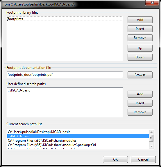
- KiCADlib.png (34.97 KiB) Viewed 6588 times
Yes I am currently in Windows

Any ideas?
Posted: 06 Jan 2013, 21:53
by Game Theory
Posted: 13 Aug 2014, 20:01
by 7bit
Most problems are solved, now just one more thing:
What do I have to send to the PCB-manufacturer?
I know that there are some gerber-files to be generated (File->Plot in pcbnew),
but what exactly do I have to send to the manufacturer and what are the settings I need?
Posted: 13 Aug 2014, 22:25
by Muirium
Submit your answers in a PERL script…
Posted: 14 Aug 2014, 09:55
by 7bit
How do I make a drill file for plated holes and one for unplated holes?
Posted: 14 Aug 2014, 10:16
by bpiphany
It may just be that you are using an archaic version of KiCAD that doesn't separate between plated and non-plated holes... In almost every case it won't matter if all holes are plated. On my first boards in KiCAD I had a semi manual emacs script to delete all plated/non-plated holes respectively before generating the drill files.
The developing versions of KiCAD has a lot of nifty new features. I don't know how much has been incorporated into the current stable version. I never had any (serious) troubles using the latest developing version. Things do change every now and then, usually to the better, but it sometimes requires some extra work to adopt projects to the new way of thinking.
Posted: 14 Aug 2014, 11:01
by 7bit
Sorry for asking, I already did this:
Code: Select all
MYNAME="$@"
MYINPUT=$MYNAME".brd"
MYPADS=$MYNAME"_pads.brd"
MYHOLES=$MYNAME"_holes.brd"

grep -cH NEWLINE $MYINPUT | grep -v \:0
grep -cH DOLLAR $MYINPUT | grep -v \:0

cat $MYINPUT |
sed 's/$/NEWLINE/' |
sed 's/^[\$]EndPAD/DOLLAREndPAD/' |
tr -d '\n' |
sed 's/NEWLINE[\$]/\n\$/g' |
grep "NEWLINEAt\([[:space:]]\+\)HOLE\([[:space:]]\+\)" -v |
sed 's/NEWLINE/\n/g' |
sed 's/DOLLAREndPAD/\$EndPAD/' | grep . > $MYPADS


cat $MYINPUT |
sed 's/$/NEWLINE/' |
sed 's/^[\$]EndPAD/DOLLAREndPAD/' |
tr -d '\n' |
sed 's/NEWLINE[\$]/\n\$/g' |
grep "NEWLINEAt\([[:space:]]\+\)STD\([[:space:]]\+\)" -v |
sed 's/NEWLINE/\n/g' |
sed 's/DOLLAREndPAD/\$EndPAD/' | grep . > $MYHOLES


echo " "
echo "output written to:"
echo "$MYPADS"
echo "$MYHOLES"
echo " "
I know this is really primitive and fails if NEWLINE or DOLLAR are in the file, or maybe if a file rm -rf is given, but no risk no fun.

Posted: 14 Aug 2014, 14:18
by Parak
My kicad version (2013-07-07 BZR 4022) automatically generates two drill files, one for plated and one for nonplated holes.
Posted: 14 Aug 2014, 14:31
by 7bit
Code: Select all
# Created by Pcbnew(2010-03-14)-final
Posted: 14 Aug 2014, 14:39
by Parak
Ew. I remember those earlier versions being quite frustrating in other ways too.
Posted: 14 Aug 2014, 15:59
by ne0phyte
7bit wrote: Code: Select all
# Created by Pcbnew(2010-03-14)-final
Why and how? That is way behind even the Debian stable repos
Posted: 14 Aug 2014, 16:10
by 7bit
Never change a running system!

Posted: 14 Aug 2014, 16:17
by ne0phyte
That only applies to software that actually works, the difference between yours and the current Kicad is quite big
