Here's the datasheet of the chip used in the M2, called EF6805U3:
https://www.digchip.com/datasheets/down ... r=EF6805U3
Unfortunately it only has the DIP package pinout, and not the PLCC one.
However, in order to guess at what is the correct PLCC pinout, let's look at a different chip in the same family that, also has a 40-pin dip variant and a 44-pin PLCC variant:
https://datasheetspdf.com/datasheet/EF6801.html
Here you can compare the DIP and PLCC packages.
You will notice that all the pins that have a functionality are in the same order when you compare DIP and PLCC packages of the same chip. This makes sense, they most likely use the same silicon die on the two chip variants, and the insides look something like this:
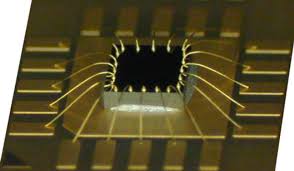
- bond_wires.jpeg (6.78 KiB) Viewed 5395 times
And while you could skip some extra pins, you really don't want to cross bond wires.
So it's a good assumption that useful pins will be in the same order on the EF6805U3 PLCC package, as in the EF6805U3 dip package. Except there will be 4 more NC (Non-connected) pins. The EF6805U3 DIP package already has an N.C. pin, so we expect to have 5 NC pins total.
We already know which is pin 1, since it's marked with a dimple.
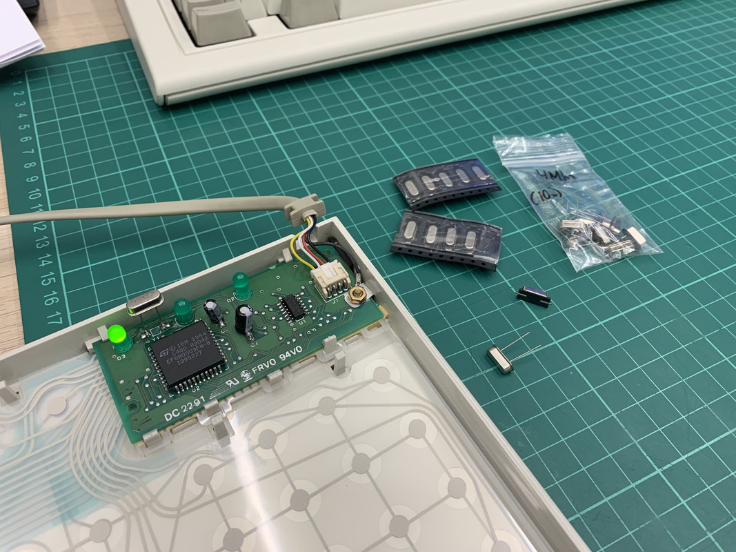
I start by putting the multimeter into continuity mode, and beeping out from gnd (the negative side of the big cap), to any pins on the chip. I have pins "1" and pin "23" beep. Pin 1 makes perfect sense, since pin 1 on the DIP also is VSS, so all okay so far. Pin 23 looks like it has a thick ground trace connected to it, and it looks intentional (i.e. it's not just thick because of an accidental ground fill), so it must be a real ground. I suppose when going from DIP to PLCC, they could have easily added ground as well instead of NC pins. So I take a note that pin 23 is Vss, and that I'm only looking for 4 more NC pins now.
I continue by beeping from Vcc (the positive side of the big cap) to any pins, and I find that pin 4 beeps. Pin 4 on the DIP package is also Vcc, it all makes sense. So therefore it must be true that pins 2 and 3 are also the same as on the DIP package, so pin 2 is ~RESET and pin 3 is ~INT.
You might notice that pin 2 (~RESET) is connected to the smaller cap's positive side. This is because the smaller cap is used as a circuit to delay the de-assertion of the microcontroller reset until the power supplies have stabilized, and the clock is running stable. In fact, in my experience this smaller cap is the one that is causing more trouble. If this cap dies then the microcontroller won't get reset properly on power-on. You can test this theory, by just quickly shorting the pins of the smaller capacitor. This will temporarly fix a misbehaving M2, until the next power cycle of the keyboard.
Now let's look for any NC pins: N.C. could be two things:
1) It could be a pin, that is connected internally to the die, and it has a function, but the function is hidden from the user. (It could be test mode functionality only used in the factory, or it could be a feature, that has been undocumented, because it didn't work right), No matter what the reason is, the expectation is that the user will leave pins as such floating.
2) True-NC pin that are actually not connected internally in the chip.
You can measure out true-NC pins, because all internally connected pins will have an ESD diode pointed from ground to the pin. So you can measure internally connected pins by putting the multimeter into diode mode, and touching the red wire to Gnd/Vss, and the black wire to the pin. If it shows a value that is not infinite, or not out-of-range, then it is a pin with some functionality. If it's not measuring anything then it's a True-NC pin.
Doing this measurement I found the following True-NC pins: 6, 20, 40.
But we were looking for 4, so it must be that we have one more non-true-NC pin.
Since this is not a true NC pin, this pin is most likely to be in the same position as on the DIP package, so right after the XTAL pin. I think this is a good assumption, but double-checking, I also tried to beep out any connections I could find between pin 8 in the PLCC package and anything else on the board, but I didn't find anything, so I think we're good.
With all of this in mind I think we're ready the draw a best-guess pinout, and it's:
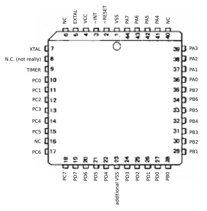
- m2_controller_guessed_chip_pintout.png (67.17 KiB) Viewed 5395 times
You will see that the white two-terminal device will connect to the XTAL and EXTAL pins.
but those bastards have three pins
The middle one of those 3 pins is probably just ground:
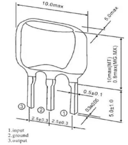
- crystal_with_ground.png (89.27 KiB) Viewed 5390 times