I'd like several pins for LEDs—think layer indicators across the number row—but that really is a 60% concern. So as long as there's enough for a 60% + 10 LEDs say. Want to be flexible for extended stuff you see. Even if it's not obvious what it is yet.
Joining split keyboard halves also comes to mind.
Can we design the teensy alternative for keyboards?
-
mohitgarg
- Main mouse: R.A.T 7
- Favorite switch: Blue
- DT Pro Member: -
That's some steller work there flasbberghast!
Before I proceed to routing,
a. Do we need the staggered pins?
b. In lieu of making the board smaller/more pins (basically more space optimized), is it an issue to have tracks (not component pads) near the mounting holes as long as there is enough clearance space (M2 screw, 4mm dia clearance). Stripping tracks from the PCb are not easy unless initiated from a connected pad. There is going to mask on the PCB.
-
Ratfink

- Location: North Carolina, USA
- Main keyboard: IBM Displaywriter
- Main mouse: CST L-Trac
- Favorite switch: Beam Spring
- DT Pro Member: -
Putting tracks near screws is a great idea, if you love shorting random tracks together when you tighten a screw!  I'd say you should try to avoid putting tracks where screw heads will go if at all possible.
-
flabbergast

- Location: Southampton, UK
- DT Pro Member: 0120
- Contact:
Staggered pins - I like them because they're great for testing without soldering. But I'm fine also with normal ones.
Traces - I'd avoid the clearance area. People can get crazy with the screws, and it puts possibly uneven pressure/tension on the area. I'd be afraid that (apart from stripping the mask) the traces may even break. A broken trace is really annoying because it sometimes works (usually when testing) sometimes not.
My own 60% PCB screw holes are visibly scratched from the screws.
@Mu: well 29 ain't enough for a normally wired 60% plus 10 LEDs (15+5+10 = 30 But for extending you usually only need 2 pins (for UART or I2C).
Traces - I'd avoid the clearance area. People can get crazy with the screws, and it puts possibly uneven pressure/tension on the area. I'd be afraid that (apart from stripping the mask) the traces may even break. A broken trace is really annoying because it sometimes works (usually when testing) sometimes not.
My own 60% PCB screw holes are visibly scratched from the screws.
@Mu: well 29 ain't enough for a normally wired 60% plus 10 LEDs (15+5+10 = 30
-
Muirium

- µ
- Location: Edinburgh, Scotland
- Main keyboard: HHKB Type-S with Bluetooth by Hasu
- Main mouse: Apple Magic Mouse
- Favorite switch: Gotta Try 'Em All
- DT Pro Member: µ
Right, but it's close. Even I don't use 10 layers! And I appreciate the desire for minimalism here. 9 extra pins is plenty for a 60% to be honest.
-
vvp

- Main keyboard: Katy/K84CS
- Main mouse: symetric 5-buttons + wheel
- Favorite switch: Cherry MX
- DT Pro Member: -
It would be better to have the left screw hole more in the centre to lessen mechanical loading.
May be you can connect the currently unused micro controller ports to 1.27 pitch pads? People who will miss a pin will like 1.27 pad more than connecting directly to a QFN pin. That is much more tricky.
May be you can connect the currently unused micro controller ports to 1.27 pitch pads? People who will miss a pin will like 1.27 pad more than connecting directly to a QFN pin. That is much more tricky.
-
Matt_
- Location: France
- Main keyboard: KBT Pure Pro
- Main mouse: G500
- Favorite switch: MX Red, MX Blue
- DT Pro Member: -
If you want a layer indicator, one RGB LED may be a good alternative to using 10 LEDs. It only needs three pins (PWM), and you can assign one color for each layer. That's what I used on my analog numpad, with one RGB LED under a windowed cap, and it worked great (you can even do that with a single pin if you use one of those smart LEDs with integrated driver).Muirium wrote: ↑Right, but it's close. Even I don't use 10 layers! And I appreciate the desire for minimalism here. 9 extra pins is plenty for a 60% to be honest.
-
Muirium
- µ
- Location: Edinburgh, Scotland
- Main keyboard: HHKB Type-S with Bluetooth by Hasu
- Main mouse: Apple Magic Mouse
- Favorite switch: Gotta Try 'Em All
- DT Pro Member: µ
Exactly. Anything that needs interpreted by the user is bullshit. If I'm in layer 4, I want a light under the 4 key. Not a code to decipher!
-
Muirium
- µ
- Location: Edinburgh, Scotland
- Main keyboard: HHKB Type-S with Bluetooth by Hasu
- Main mouse: Apple Magic Mouse
- Favorite switch: Gotta Try 'Em All
- DT Pro Member: µ
Seeing as blue is completely unacceptable at night, when I'm dozy and indicators are most useful, that limits colours a bit. Besides, such cheaping/lazy way out on a custom board is fundamentally wrong, to my picky mind!
-
vvp
- Main keyboard: Katy/K84CS
- Main mouse: symetric 5-buttons + wheel
- Favorite switch: Cherry MX
- DT Pro Member: -
Murium, if you want a layer indicator then it is better to have 7-segment LED display instead of LEDs next to a numerical keycap. The point is that you will see the layer number clearly even when it is dark to see the keycap legends.
http://sk.farnell.com/broadcom-limited/ ... 0019/false
It is even better to add alphanumeric display and show layer name instead of a number.
http://sk.farnell.com/broadcom-limited/ ... 0019/false
It is even better to add alphanumeric display and show layer name instead of a number.
-
Matt_
- Location: France
- Main keyboard: KBT Pure Pro
- Main mouse: G500
- Favorite switch: MX Red, MX Blue
- DT Pro Member: -
I can't stand blue LEDs either, but as soon as you mix blue with another color the annoyance disappears. But that was just a suggestion to save pins, and since it looks like there will be lots of extras with a 60% matrix there is no point in debating over it. Sorry for derailing the threadMuirium wrote: ↑Seeing as blue is completely unacceptable at night, when I'm dozy and indicators are most useful, that limits colours a bit. Besides, such cheaping/lazy way out on a custom board is fundamentally wrong, to my picky mind!
-
flabbergast
- Location: Southampton, UK
- DT Pro Member: 0120
- Contact:
We can move the left mounting hole more further up, if we split the two innermost pads (3rd column; SWD debug pads) apart from each. That should not be a problem; routing will get more interesting, but likely doable.
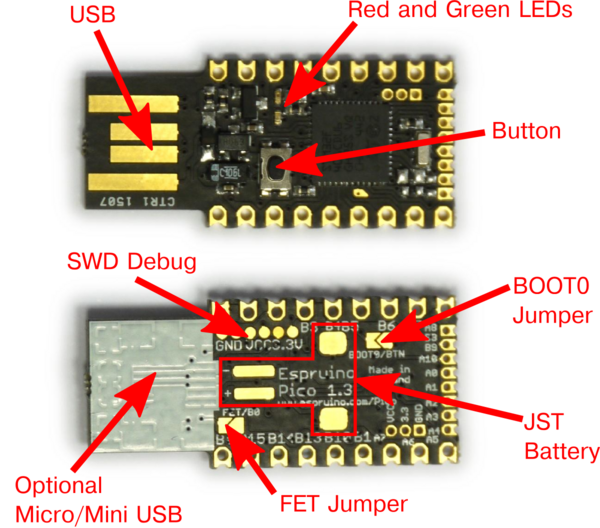
The remaining MCU lines - there's 5 of them. I think it's good call to try to bring them out to pads. For 3 of them it's no problem to add pads like the ones called "SWD Debug" on this picture {2 will be on the left of the MCU, one on the right}. However for the remaining 2 it is really tricky - these are two in the middle of the "power side" (PTE20 and PTE21)... I probably won't be able to do this without a more substantial moving the components around.
The remaining MCU lines - there's 5 of them. I think it's good call to try to bring them out to pads. For 3 of them it's no problem to add pads like the ones called "SWD Debug" on this picture {2 will be on the left of the MCU, one on the right}. However for the remaining 2 it is really tricky - these are two in the middle of the "power side" (PTE20 and PTE21)... I probably won't be able to do this without a more substantial moving the components around.
-
jacobolus
- Location: geekhack ergonomics subforum
- Favorite switch: Alps plate spring; clicky SMK
- DT Pro Member: -
Incorrect. Blue LEDs and “white” LEDs (blue LED + yellow phosphor) are terrible at night, irrespective of other combined light sources: they wipe out your night vision (it takes at least 20–30 minutes to adapt back to dark afterward), and they disrupt sleep cycles. (Fluorescent bulbs are also pretty bad; I’m an equal-opportunity short-wavelength-emitting-lamp hater.)Matt_ wrote: ↑I can't stand blue LEDs either, but as soon as you mix blue with another color the annoyance disappears.
They’re terrible in LED streetlamps. They’re terrible in LED car headlamps. They’re terrible in LED flashlights and camping lanterns (ugh, those LED lanterns are the fucking worst). They’re terrible in LED lamps on the nightstand. Etc.
When I walk my dog around the recently-LED-illuminated neighborhood at night, I’ve taken to wearing orange safety glasses – makes a big improvement. My wifi router, which is most convenient to locate in the bedroom, has stupid flickering blue LEDs to signal network activity; fortunately heavily marking them with a black sharpie cuts out most of the light,
Laptops and phones and televisions with LED backlight are also terrible at night, anytime within ~2 hours of bedtime. At least install f.lux on those babies, and turn the brightness all the way down.
LEDs are fine for daytime office lighting though.
Last edited by jacobolus on 05 May 2016, 19:10, edited 1 time in total.
-
matt3o

- -[°_°]-
- Location: Italy
- Main keyboard: WhiteFox
- Main mouse: Anywhere MX
- Favorite switch: Anything, really
- DT Pro Member: 0030
- Contact:
this is very interesting and within my field of expertiseflabbergast wrote: ↑Finally I've just found out on the web that someone wanted to make a chrome plugin that could flash the chip directly from the browser (supposed to be possible using chrome HID api and the fact that the bootloader on this thing is also HID). I don't think he finished the project, so at this moment it's just a possibility (which is way out of my comfort zone, so I can't tell if it's possible or not).
-
matt3o
- -[°_°]-
- Location: Italy
- Main keyboard: WhiteFox
- Main mouse: Anywhere MX
- Favorite switch: Anything, really
- DT Pro Member: 0030
- Contact:
PS: I created the elf-io entity on github https://github.com/elf-io I'd like to post everything about this board there (already invited flabbergast). I don't like github wiki so I'll probably set a docuwiki or something on elf.io.
-
Matt_
- Location: France
- Main keyboard: KBT Pure Pro
- Main mouse: G500
- Favorite switch: MX Red, MX Blue
- DT Pro Member: -
Yeah, I'm aware of those issues. It's just that, regardless of health hazards, for me blue LEDs always feel like a stab in the eye (even in daylight), yet that sensation disappears when the blue is mixed with another color, in which case it's not more problematic that the big screen shining in front of my eyes. But then again we're way OT here, maybe we should discuss the matter in another thread?jacobolus wrote: ↑Incorrect.
On the one hand it would be nice to have more lines brought out to pads, on the other not everyone will be willing to solder wires to these tiny pads, so even if they are here they may be less used than regular pads. I'd say, try to do your best with the available space, but don't sacrifice more important design features (better routing or component placement for instance) just for those two extra lines.flabbergast wrote: ↑The remaining MCU lines - there's 5 of them. I think it's good call to try to bring them out to pads. For 3 of them it's no problem to add pads like the ones called "SWD Debug" on this picture {2 will be on the left of the MCU, one on the right}. However for the remaining 2 it is really tricky - these are two in the middle of the "power side" (PTE20 and PTE21)... I probably won't be able to do this without a more substantial moving the components around.
-
matt3o
- -[°_°]-
- Location: Italy
- Main keyboard: WhiteFox
- Main mouse: Anywhere MX
- Favorite switch: Anything, really
- DT Pro Member: 0030
- Contact:
was wondering, should we give an option to power the board externally (ie: not from USB)?
-
mohitgarg
- Main mouse: R.A.T 7
- Favorite switch: Blue
- DT Pro Member: -
I would keep all "extra" functionality on separate modules, perhaps, we can develop this as a system.matt3o wrote: ↑was wondering, should we give an option to power the board externally (ie: not from USB)?
- Main MCU
- LED Controller
- Wireless Module
- I/O expander
..etc
-
matt3o
- -[°_°]-
- Location: Italy
- Main keyboard: WhiteFox
- Main mouse: Anywhere MX
- Favorite switch: Anything, really
- DT Pro Member: 0030
- Contact:
well "power" is a bit of beast of its own. the MCU has to be powered somehow
-
flabbergast
- Location: Southampton, UK
- DT Pro Member: 0120
- Contact:
I already thought about this (hence the solder jumper), but looking at the datasheet the way I thought about it may not be the best. I'll report.matt3o wrote: ↑was wondering, should we give an option to power the board externally (ie: not from USB)?
@Matt_: about extra pads: the discussion was about those that I couldn't bring out to normal through-hole pads. So this is something extra, no impact on the current status.
@matt3o: HID bootloader protocol description: the best I can do right now is datasheet, section "13.4.3.4 HID reports" for the HID protocol specifics, section "13.3.8 Bootloader Command API" for the actual API {one layer higher after talking over HID is sorted out}.
-
flabbergast
- Location: Southampton, UK
- DT Pro Member: 0120
- Contact:
OK, getting my head around the power options. Use cases:
1) Default: powered from USB, MCU provides 3.3V regulated (120mA max including the MCU)
2) Powered externally with >= 3.6V (e.g. LiPo). MCU provides 3.3V regulated. Optional charger hookable. USB working.
3) Powered externally with <= 3V (e.g. 2 AA). No charger.
Doing more than 1) will require some changes. I would like to make 1) and 2) possible {the charger would be a daughter board that's possible to hook next to this one on the left}. Visible changes:
- move the RESET line from a through-hole pad to a SMT pad {I think this if fine, this pad is really useful only for wiring an external reset button, which happens pretty rarely, and then it's possible to use the SMT pad.}
3) will be possible automatically (it is even now), provided that USB is not used at all. To make it work also with USB (e.g. normally battery powered but when plugged into USB it will act as a USB device) will require one more solder jumper; and since I don't want to sacrifice any more through-hole pads, I would only make a SMT pad to wire the battery to (on the bottom side).

-
vvp
- Main keyboard: Katy/K84CS
- Main mouse: symetric 5-buttons + wheel
- Favorite switch: Cherry MX
- DT Pro Member: -
Nice, and you have all the pins there. Very cool
I have the same complain though: It would be good if the screw hole below USB connector can be moved "up" more to the centre of the board. The reason is that if a force from the PCB back to its front is exerted from the USB cable then there will be bigger leverage (from the screw hole to the bottom edge of the PCB) to counter it and therefore less stress on the PCB and screw. The ideal position for a screw hole is in the centre between top and bottom edge.
If the mounting holes are used then the PCB should be supported around its edges by the case.
-
matt3o
- -[°_°]-
- Location: Italy
- Main keyboard: WhiteFox
- Main mouse: Anywhere MX
- Favorite switch: Anything, really
- DT Pro Member: 0030
- Contact:
that sounds totally fine to meflabbergast wrote: ↑ - move the RESET line from a through-hole pad to a SMT pad {I think this if fine, this pad is really useful only for wiring an external reset button, which happens pretty rarely, and then it's possible to use the SMT pad.}
the board is so small that honestly I believe anywhere you put the screws will be finevvp wrote: ↑I have the same complain though: It would be good if the screw hole below USB connector
-
flabbergast
- Location: Southampton, UK
- DT Pro Member: 0120
- Contact:
Nice, Mohit!
Unaware that you're working, I've made some changes (pushed to github now) to accomodate the power options... I'm sorry about that (I know I said the schematic is correct...) so our changes will need to be merged somehow if we decide to implement both.
There's a couple of things:
- the big QFN pad will need to be stitched to the bottom ground plane by vias for thermal relief (not done yet)
- gotta be careful when routing D+/D- : it's a differential pair so the traces should be as similar as possible (along each other, same number of vias, etc...) {I think your routing should be fine though.}
- I personally like to route the power lines with 10mil traces. I don't think that's really necessary, but just to be on the safe side.
-
vvp
- Main keyboard: Katy/K84CS
- Main mouse: symetric 5-buttons + wheel
- Favorite switch: Cherry MX
- DT Pro Member: -
flabbergast: Do you have some articles about how important the balancing of the differential pair is for half and full speed devices? The lines are not very balanced from the beginning because one of them is pulled up with 1k5 resistor (to indicate the USB device is connected). Also I saw a lot of USB devices which just had few cm of free unshielded wires between the cable and the PCB. Far from a proper differential pair but, yeah, their length was about the same. This is not to say that we should not try to keep the lines the same as much as possible. I'm just curious how important it is for half and full speed devices.
matt3o: The smaller the board is the bigger the forces on the screw are. At the current position, the forces are about 1.6 times bigger compared to the position in the centre. If we are putting the screw holes there at all (and because of that we have bigger troubles to route it and provide all the pins) then we at least should place them as well as possible. Notice the forces can be quite big because they will be cumming from the USB cable.
matt3o: The smaller the board is the bigger the forces on the screw are. At the current position, the forces are about 1.6 times bigger compared to the position in the centre. If we are putting the screw holes there at all (and because of that we have bigger troubles to route it and provide all the pins) then we at least should place them as well as possible. Notice the forces can be quite big because they will be cumming from the USB cable.
-
Wodan

- ISO Advocate
- Location: ISO-DE
- Main keyboard: Intense Rotation!!!
- Main mouse: Logitech G903
- Favorite switch: ALL OF THEM
- DT Pro Member: -
I often desoldered the controller from a vintage keyboard, soldered in some male headers and just placed the teensy in the position of the old controller. It's DIP form factor saved me alot of soldering work there.
The fact that the GND/5V pins were part of the DIP rows limited the possibilities here, still I would love to see a controller that maintains two rows of pins that will fit on a row of DIP headers. This is also a very convenient way to fix the controller.
The latest design looks like there's ALOT of pins available but also alot of hand wiring required.
-
flabbergast
- Location: Southampton, UK
- DT Pro Member: 0120
- Contact:
@Wodan: Having DIP rows would mean the USB connector has to be on a shorter side. I am actually very surprised you even found one keyboard which is sufficiently pin- and size- compatible with a Teensy...
@Mohit: also I think that for M2.5 screws we should do 5mm dia clearance.
@vvp: I don't really have any articles; and I did try myself doing USB 1.1 where a part of the routing was on a breadboard, like this. So I don't think we can go 'unusably wrong', just that we should try our best. We already do no satisfy some of the recommendation from the spec.